525-2102-2 Circuit Frame
Circuit Frames provide a reliable method for replacing damaged surface mount pads, lands, and conductors on circuit boards. Featuring a dry-film adhesive backing, they bond quickly using heat from a Bonding Iron or Bonding System, eliminating the need for liquid epoxies. The resulting bond strength matches the original conductor and follows IPC-recommended repair procedures.
Trusted for more than 40 years, Circuit Frames are widely used by commercial, medical, and military manufacturers for high-reliability circuit board rework and repair applications. If you require a custom shape, submit a request using our Contact Us form.
|
| Shapes and Pattens |
| - |
Qty |
Shapes, Patterns Included |
| - | Qty | Shapes, Patterns Included |
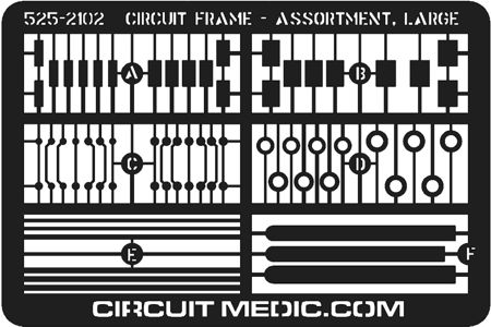
| A | 9 | SMD Pads 0.040" x 0.120" (1.00 mm x 3.08 mm) |
| A | 8 | SMD Pads 0.060" x 0.120" (1.52 mm x 3.08 mm) |
| B | 8 | SMD Pads 0.080" x 0.120" (2.03 mm x 3.08 mm) |
| B | 7 | SMD Pads 0.090" x 0.120" (2.28 mm x 3.08 mm) |
| C | 10 | BGA Pads 0.030" (0.76 mm) Diameter |
| C | 10 | BGA Pads 0.035" (0.89 mm) Diameter |
| C | 18 | BGA Pads 0.040" (1.00 mm) Diameter |
| D | 5 | PTH Lands 0.080" OD x 0.050" ID (1.27 mm OD x 1.27 mm ID) |
| D | 4 | PTH Lands 0.090" OD x 0.055" ID (1.52 mm OD x 1.40 mm ID) |
| D | 7 | PTH Lands 0.100" OD x 0.060" ID (1.78 mm OD x 1.52 mm ID) |
| E | 1 | Conductors 0.015" (0.38 mm) wide |
| E | 2 | Conductors 0.020" (0.51 mm) wide |
| E | 2 | Conductors 0.025" (0.63 mm) wide |
| F | 1 | Edge Contacts .070" (1.78 mm) wide |
| F | 1 | Edge Contacts .080" (2.03 mm) wide |
|
| Base Material Specifications |
| Overall Frame Size |
2.25" x 1.50" (57 x 38 mm) |
| Base Material |
Rolled Annealed Copper Foil, UNS C11000 (Alloy C110), ASTM B152, IPC-4562A, 0.0014 in (0.036 mm) thick. |
| Plating |
.0001" (.0025 mm) 63/37 Tin/Lead, Non RoHS Compliant
|
| Surface Treatments |
Top side plated. Bottom side treated to promote adhesion. |
| Shelf Life |
Shelf life of base material without adhesive application is unlimited. |
| RoHS and REACH |
CircuitMedic Circuit Frames contain less than 0.1% by weight any substance listed as a very high concern in Article 59 of REACH. |
| Adhesive Backing Specifications |
| Adhesive Backing |
Optional adhesive backing film is applied using a quick-bond process that retains B-staged adhesive properties. |
| Adhesive Material |
B-staged modified acrylic film adhesive .002" (.051 mm) thick. |
| Certification |
Adhesive backing is certified to IPC-4203/18: Adhesive Coated Dielectric Films for Use as Cover Sheets for
Flexible Printed Circuitry and Flexible Adhesive Bonding Films.
|
| Solder Resistance |
Passes IPC-TM-650, 2.4.13 Solder Float Resistance 10 seconds at 288°C (550°F). |
| Bonding Temperature |
475°F ± 25°F (246°C ± 14°C) |
| Bonding Pressure |
200 - 400 psi (14-28 kg/cm2) |
| Bonding Time |
30 seconds |
| Peel Strength |
Minimum 8 lbs/inch (1.43 kg/cm) after cure to FR-4 material. |
| Outgassing |
The Bonding Film used on Circuit Frames consistently meet the criteria for NASA applications. Maximum 1.0% TML and a Maximum 0.10% CVCM.
Samples have been submitted for testing to Goddard Space Flight Center and other facilities, and the results are; Data Reference: GSC 17366; %TML: 0.94%; %CVCM: 0.06%
|
| Shelf Life |
One year minimum. Each Circuit Frame package is stamped with the expiration date. Adhesive material is sensitive to light and heat.
Store in a dark or refrigerated environment to preserve the shelf life.
|
|
| Classifications |
| Harmonize Code |
7410.21.6000 |
| Export Administration Regulations (EAR) |
EAR99 |
| Export Control Classification Number (ECCN) |
Not Applicable |
|
|