CircuitMedic
First-Aid Kits for Circuit Boards®
A Circuit Technology Center Company
Haverhill, MA 01835 USA
www.circuitmedic.com

Circuit Frames

[unknown placeholder $article.title$]
Circuit Frames are used to replace damaged surface mount pads, lands, and conductors without the mess of liquid epoxy, with bond strength equal to the original, in just a few minutes. Circuit Frames with dry-film adhesive backing make this delicate repair procedure easy, fast, and highly reliable. This reliable IPC-recommended procedure meets the highest conformance level for this type of repair. For over 30 years, Circuit Frames have been used by thousands of high-reliability manufacturers around the globe.
Ordering
Part No. Description Part No. Description
525-2201-1 Circuit Frame, Blank, Bright Tin Plated 525-2301-1 Circuit Frame, Conductors, Bright Tin Plated
525-2901-3 Circuit Frame, Edge Contacts, Nickel/Gold Plated 525-2101-1 Circuit Frame, Assortment, Bright Tin Plated
525-2102-1 Circuit Frame, Assortment, Bright Tin Plated 525-2601-1 Circuit Frame, Lands/Pads, Bright Tin Plated
525-2401-1 Circuit Frame, SMD Pads, Bright Tin Plated 525-2701-1 Circuit Frame, BGA Pads, Bright Tin Plated
525-2402-1 Circuit Frame, SMD Pads, Bright Tin Plated 525-2101-2 Circuit Frame, Assortment, Tin/Lead Plated
525-2102-2 Circuit Frame, Assortment, Tin/Lead Plated 525-2201-2 Circuit Frame, Blank, Tin/Lead Plated
525-2301-2 Circuit Frame, Conductors, Tin/Lead Plated 525-2401-2 Circuit Frame, SMD Pads, Tin/Lead Plated
525-2402-2 Circuit Frame, SMD Pads, Tin/Lead Plated 525-2601-2 Circuit Frame, Lands/Pads, Tin/Lead Plated
525-2701-2 Circuit Frame, BGA Pads, Tin/Lead Plated
CircuitMedic
First-Aid Kits for Circuit Boards®
A Circuit Technology Center Company
Haverhill, MA 01835 USA
www.circuitmedic.com

Circuit Frames

Adhesive Backing Specifications
Adhesive Backing The adhesive backing film is applied to the copper base material using a quick-bond process that retains B-staged adhesive properties.
Adhesive Material B-staged modified acrylic film adhesive .002" (.051 mm) thick.
Certification Adhesive backing is certified to IPC-4203/18: Adhesive Coated Dielectric Films for Use as Cover Sheets for Flexible Printed Circuitry and Flexible Adhesive Bonding Films.
Solder Resistance Passes IPC Spec 10 sec at 288°C (550°F).
Bonding Temperature 475°F ± 25°F (246°C ± 14°C)
Bonding Pressure 200 - 400 psi (14-28 kg/cm2)
Bonding Time 30 seconds
Peel Strength Minimum 8 lbs/inch (1.43 kg/cm) after curing to FR-4 material.
Outgassing The Bonding Film used on Circuit Frames consistently meets the criteria for NASA applications. Maximum 1.0% TML and a Maximum 0.10% CVCM. Samples have been submitted for testing to Goddard Space Flight Center and other facilities, and the results are; Data Reference: GSC 17366; %TML: 0.94%; %CVCM: 0.06%
Shelf Life One year minimum. Each Circuit Frame package is stamped with the expiration date. The adhesive material is sensitive to light and heat. Store in a dark or refrigerated environment to preserve the shelf life.
Plating Options
Bright Tin .0001" (.0025 mm) Bright Tin (Lead-Free), RoHS Compliant
Tin/Lead .0001" (.0025 mm) 63/37 Tin/Lead, Non RoHS Compliant
Nickel/Gold .000050" (.00127 mm) Gold over .000100" (.00254 mm) Nickel, RoHS Compliant
CircuitMedic
First-Aid Kits for Circuit Boards®
A Circuit Technology Center Company
Haverhill, MA 01835 USA
www.circuitmedic.com

Circuit Frames

Circuit Frame Repair/Replacement Procedure

Circuit Frame
Figure 1.
1. Remove the defective pad, land, or conductor. If a connecting circuit is on the circuit board surface, apply liquid flux and tin it with solder. See Figure 1.

2. If the base material is severely damaged, it may need to be repaired before replacing the new pad. See baseboard repair procedures at www.circuitrework.com/guides/guides.html.

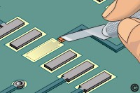
3. Select a replacement pad, land, or edge contact from a Circuit Frame. Carefully scrape off the adhesive film from the solder joint area, then trim it out. See Figure 2.
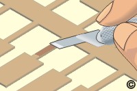
Circuit Frame
Figure 2.
4. Clean the area, then place the new circuit in position using high-temperature tape. Check to be sure the new circuit is properly aligned. See Figure 3.

5. Select a Bonding Tip with a bottom surface that closely matches the shape of the new circuit. Insert the Bonding Tip into the Bonding Iron. Allow time for the tip to heat up to the proper temperature, 480°F +/- 25°F (250°C +/- 14°C).

Circuit Frame
Figure 3.
6. Apply light, even perpendicular pressure to the surface of the high-temperature tape for 5 seconds using the Bonding Iron. The heat transmits through the tape to quickly tack the new circuit in place.

7. Carefully remove the high-temperature tape leaving the circuit in position.

8. Apply heat a second time using the Bonding Iron directly to the top surface of the new circuit. Apply light even perpendicular pressure for 30 seconds to permanently cure the adhesive.

Circuit Frame
Figure 4.
9. If the new pad has a connecting circuit, apply liquid flux and the lap solder the connection. See Figure 4.

10. Mix epoxy and coat the lap solder joint connection area if desired.